Tidying the Main Circuit
The top-level schematic was getting a bit cluttered, so I moved some of the logic into subcircuits.
- Main memory address multiplexing
- Register file address multiplexing -- incorporated into the RF Address Incrementer subcircuit
- Bit address multiplexing -- incorporated into the Bit Counter subcircuit
- ALU input selection
- Microcode branching -- combined with the State Counter and renamed to State Control
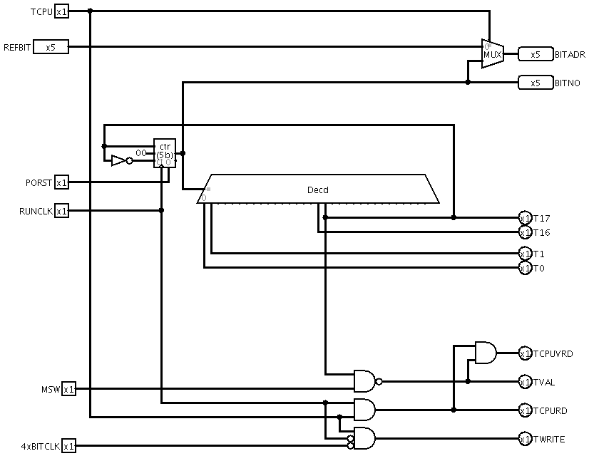
- Bit Counter -- now Bit Timing, incorporates more timing signal generation logic
Also, the latches before the inputs to the ALU have been moved back
into the register file subcircuit. This uses more latches, but has the
advantage that the signals going to the ALU input selection network are
stable instead of flipping between CPU and display refresh values,
which makes troubleshooting easier.
Change to Run Control
While tidying up, I managed to break the Halt
instruction, and this led me to discover a drawback in my
implementation of Single Clock mode. The way I had it, when in Single Clock
mode, the Run FF was set for one BITCLK cycle and then cleared.
However, this made it difficult to debug the Halt instruction by
stepping in Single Clock mode, because I couldn't distinguish between
then Run FF being cleared by the Halt instruction and by the Single
Clock mechanism.
So I modified the Run Control subcircuit slightly. Instead of feeding
into the Stop logic, the Single Clock mode input now simply freezes
RUNCLK in the same way that UBREAK does. The Run FF remains set, and a
single RUNCLK pulse is allowed through each time CONTINUE is pressed.
As part of this change, the gate for enabling RUNCLK has been moved from the top level into Run Control.
Updated Schematics
Top Level

Run Control

Bit Counter

Register File Address Generator (formerly Register File Address Incrementer)

ALU Input Select

State Control (formerly State Counter)

Bit Timing (formerly Bit Counter)