Registers and ALU

Register File

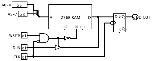
There will eventually be two of these, one holding the Accumulator and Multiplier Registers (which won't need to be accessed at the same time) and one holding the Product Register.


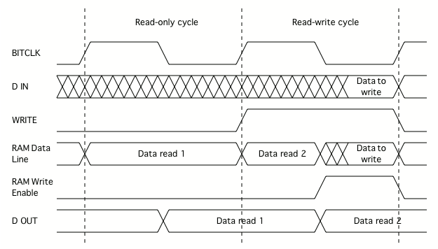
This subcircuit incorporates logic to support the division of each bit period into a Read and a Write phase. Data is read from the RAM when the clock is high and latched into the output flip-flop on the falling edge of the clock. Writing to the RAM is enabled when the WRITE control input is active and the clock is low.

ALU

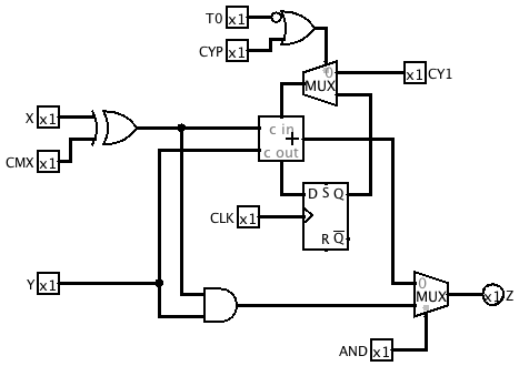
The ALU is built around a one-bit full adder with a flip-flop to hold the carry between bits. Additional logic allows one of the inputs to be complemented (CMX = 1), and a logical AND operation to be selected instead of the adder output (AND = 1).


The CYP and CY1 inputs control the carry input to the adder during T0. When CYP = 0, the carry in is equal to CY1, otherwise the carry out from the previous cycle is used. During all other bit times, the carry out from the previous bit is used.

Useful combinations of control inputs include:

CYP
CY1
CMX
AND
Result
0
0
0
0
Y + X
0
1
0
0
Y + X + 1
1
x
0
0
Y + X with carry in
0
1
1
0
Y - X
0
0
1
0
Y - X - 1
1
x
1
0
Y - X with carry in
x
x
x
1
Y AND X

Updated Main Circuit

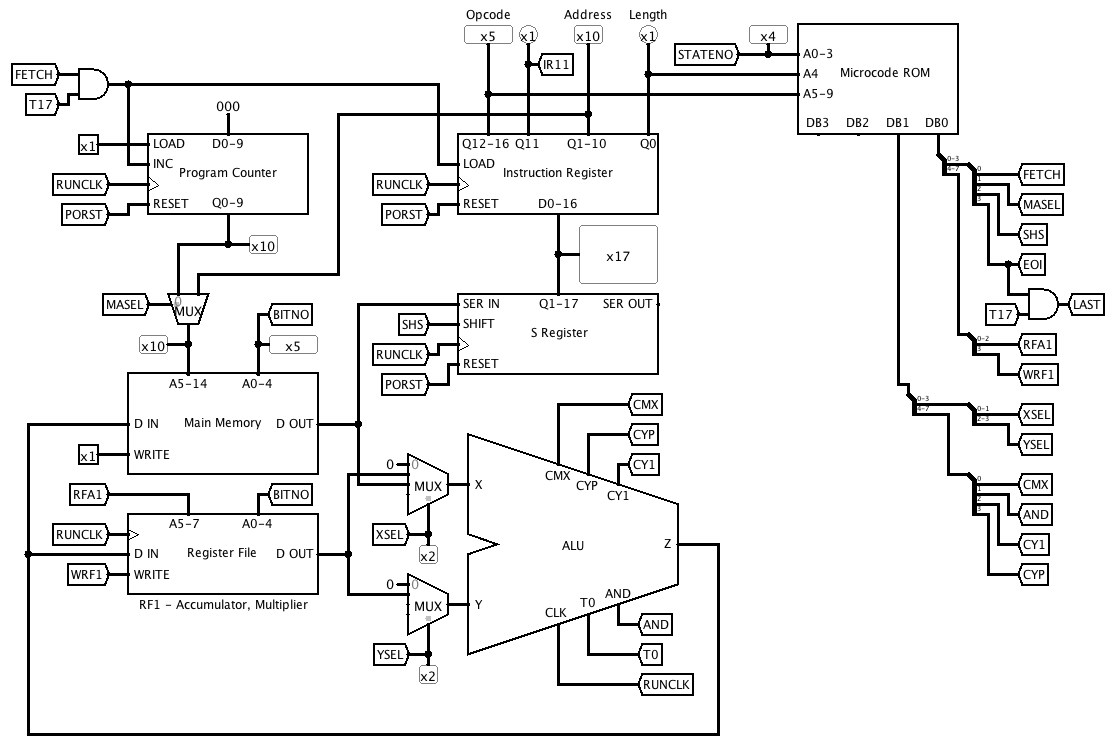
Here's the main circuit with the ALU and one of the register files added.


The following microinstruction fields have also been added:

EOI End of Instruction
Indicates the last short word cycle of an instruction. Causes LAST to be activated during T17.
RFA1
Register File 1 Address
Selects one of 8 short words in Register File 1.
WRF1
Write Register File 1
Causes the output of the ALU to be written into Register File 1.
XSEL
X Select
Selects the source for ALU input X.
YSEL
Y Select
Selects the source for ALU input Y.
CMX
Complement X
ALU control inputs
AND
Logical AND
CY1
Carry in value
CYP
Use previous carry

XSEL values:

00
Constant 0
01
Register File 1
10
Main Memory
11
Currently unused

YSEL values:

00
Constant 0
01
Register File 1
10
Currently unused
11